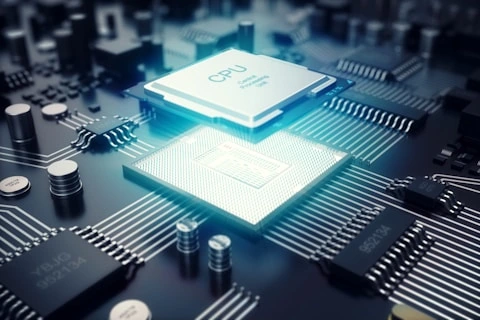
AI and High-Performance Computing (HPC)
Advanced nodes enable computationally heavy workloads with reduced latency and improved power efficiency.
Semiconductors are the invisible engines powering the digital transformation era. From smartphones and cloud data centers to autonomous vehicles and IoT devices, integrated circuits (ICs) form the backbone of modern technology. The evolution of semiconductor process nodes has enabled this transformation by consistently reducing transistor sizes, thereby increasing transistor density, improving performance, and lowering power consumption. Notably, semiconductor manufacturing has followed Moore's Law for decades, doubling the number of transistors approximately every two years. However, as we enter the sub-5nm era, both technical and economic challenges reshape how the industry innovates.
The term process node historically referred to the physical gate length of transistors. Today, however, it is largely a marketing term denoting minimum feature sizes, gate pitch, or metal pitch, which vary across foundries. Despite this shift, process nodes remain central to semiconductor manufacturing, directly influencing transistor density, power efficiency, and performance gains. Advanced architectures such as Fin Field Effect Transistors (FinFETs) and Gate-All-Around FETs (GAAFETs) optimize current flow and switching speeds.
90nm
~2004
Copper interconnects, Low-k dielectrics
~100
Enhanced leakage control
45nm
~2007
High-k metal gates
~300
Improved power efficiency
22nm
~2011
3D Tri-gate transistors
~900
FinFET adoption
7nm
~2018
EUV lithography
~137 million
Extreme Ultraviolet (EUV) introduction
5nm
~2020
Advanced FinFET, EUV
~173 million
Higher density + AI acceleration
3nm & below
2023–2025
GAAFETs, nanosheets
~220+
New transistor architectures
Transitioning from 90nm to 5nm, manufacturers achieved nearly a 75% reduction in feature size and more than a 1000% increase in transistor density, demonstrating the exponential trajectory of semiconductor progress.
Advanced nodes enable computationally heavy workloads with reduced latency and improved power efficiency.
Ultra-small process nodes facilitate low-power, high-performance chips critical for edge devices and IoT ecosystems.
With the rise of autonomous vehicles, chips manufactured at advanced nodes are indispensable for safety-critical real-time systems.
The cost per wafer at sub-5nm nodes increases significantly, raising barriers to entry for smaller fabs.
The 5nm node is not the end of Moore's Law, but rather an inflection point. Emerging solutions include:
The evolution of semiconductor process nodes is a testament to human ingenuity in pushing the limits of physics and manufacturing. While Moore's Law may be slowing, innovation in device architecture, lithography techniques like EUV, and advanced packaging continues to drive progress. Ultimately, semiconductors remain the cornerstone of digital transformation, underpinning industries from consumer electronics to AI-driven automation. As we move beyond 5nm, the semiconductor industry stands at the crossroads of technological breakthroughs and economic constraints, ensuring that the journey of integrated circuits remains as dynamic as ever.
A semiconductor process node refers to the size of the features in a chip's design, such as the transistor gate length or metal pitch. While initially tied to physical dimensions, today it largely represents a technology generation, reflecting improvements in transistor density, power efficiency, and performance.
The evolution of semiconductors is marked by continual scaling of transistors, from micrometer-sized features to nanometer and now angstrom-level processes. This has enabled higher computational performance, lower power consumption, and applications ranging from personal electronics to AI supercomputing.
Technology nodes have evolved from 90nm to 5nm and beyond, incorporating innovations such as High-k metal gates, FinFETs, EUV lithography, and GAAFETs. Each node represents a leap in transistor density and efficiency, driving the semiconductor industry forward.
The 8 primary processes in semiconductor manufacturing include: 1. Wafer Preparation, 2. Oxidation, 3. Lithography, 4. Etching, 5. Doping (Ion Implantation), 6. Deposition, 7. Metallization (Interconnects), 8. Packaging and Testing. These processes collectively enable the creation of integrated circuits at increasingly smaller technology nodes.